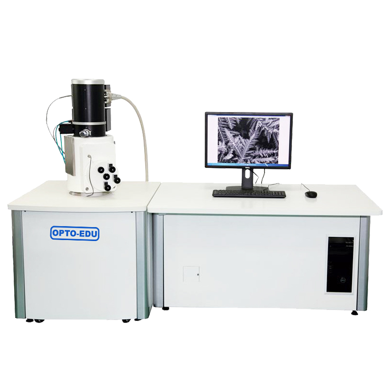
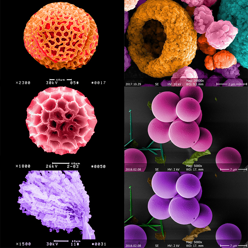
A63.7080 Schottky Field Emission Gun Scanning Electron Microscope, SED+CCD, 8x~800000x, 5 Axes Auto Middle Stage

  • 8x~800000x With Detector SED+CCD, Five Axes Manual Stage or Motorized Stage
  • E-Beam Acceleration With Stable Beam Current Supply Excellent Image Under Low Voltage
  • Non Conduction Sample Can Be Observed Directly No Need To Be Sputtered In Low Voltage
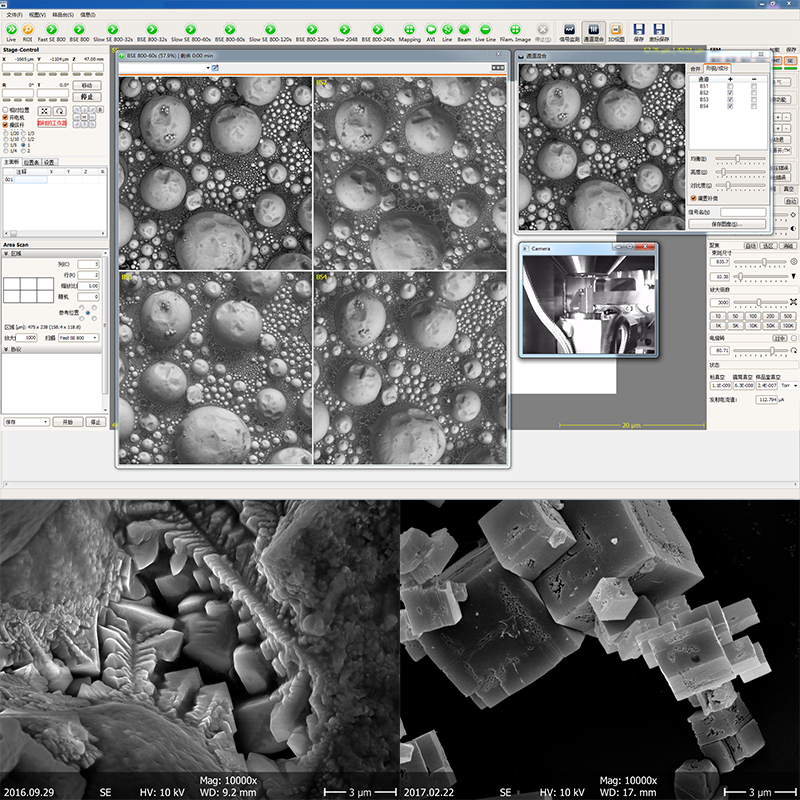
  • Easy & Friendly Operation Interface, All Controled By Mouse In Windows System
  • Large Sample Room With Five Axes Eucentric Motorized Stage Large Size, Max Specimen Dia.175mm

Products Details

A63.7080, A63.7081 Software Main FunctionHigh voltage integrated commissioningAutomatic filament on / offPotential shift regulationBrightness adjustmentElectric to central adjustmentAutomatic brightnessContrast adjustmentObjective lens adjustmentAuto focusMagnification adjustmentObjective degaussingAutomatic astigmatism eliminationSelected area scanning modeElectric rotation adjustmentManagement of microscope parametersPoint scanning modeElectron beam displacement adjustmentReal time display of scanning field sizeLine scanning modeElectron beam tilt adjustmentGun lens adjustmentSurface scanningScanning speed adjustmentMultichannel inputHigh voltage power monitoringSwing centeringRuler measurement
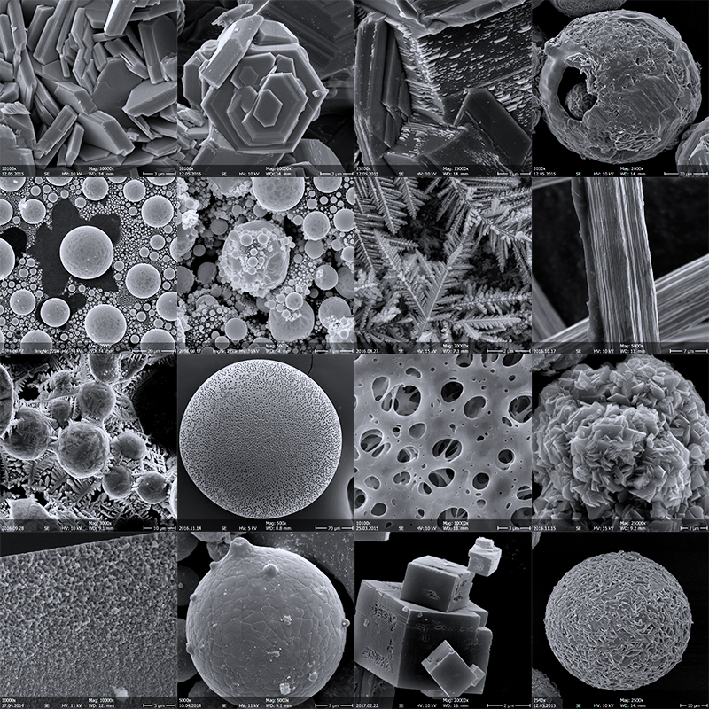
A63.7080-01 A63.7080-02 A63.7080-03 A63.7080-04 A63.7080-05 A63.7080-06 A63.7080-07 A63.7080-08 A63.7080-09 A63.7080-10 A63.7080-11 A63.7080-12 A63.7080-13 A63.7080-14 A63.7080-15
SEM A63.7069  A63.7080 A63.7081
Resolution 3nm@30KV(SE)6nm@30KV(BSE) 1.5nm@30KV(SE)3nm@30KV(BSE) 1.0nm@30KV(SE)3.0nm@1KV(SE) 2.5nm@30KV(BSE)
Magnification 8x~300000x Negative True Magnification 8x~800000x Negative True Magnification 6x~1000000x Negative True Magnification
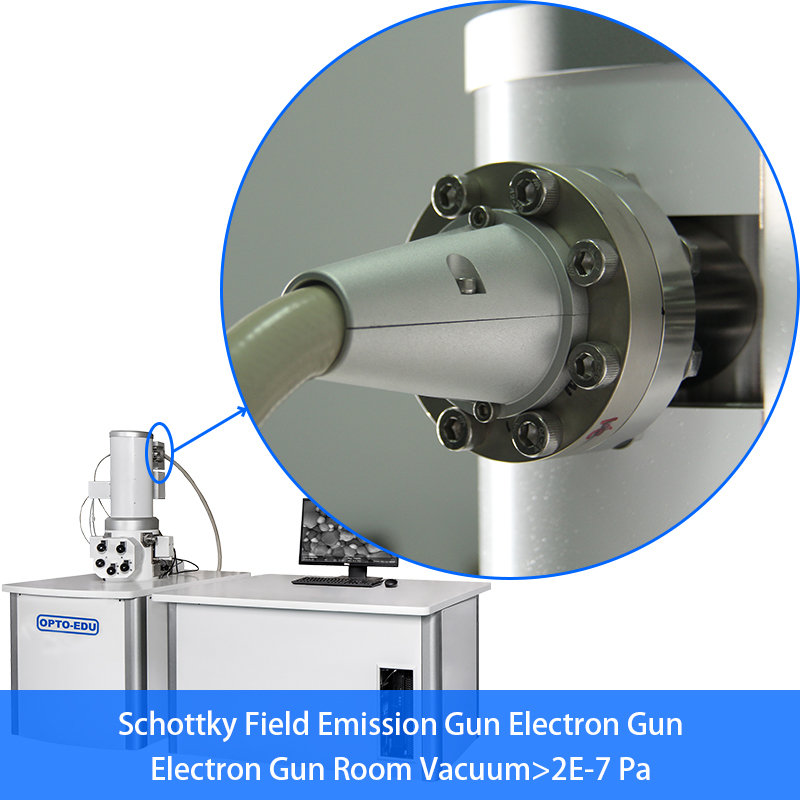
Electron Gun Pre-Centered Tungsten Filament Cartridge Schottky Field Emission Gun Schottky Field Emission Gun
Voltage Accelerating Voltage 0~30KV, Continuous Adjustable, Adjust Step 100V@0-10Kv, 1KV@10-30KV 
Quick View One Key Quick View Image Function N/A N/A
Lens System Three-levels Electromagnetic Tapered Lens Multi-levels Electromagnetic Tapered Lens
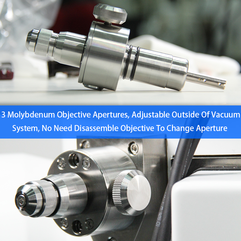
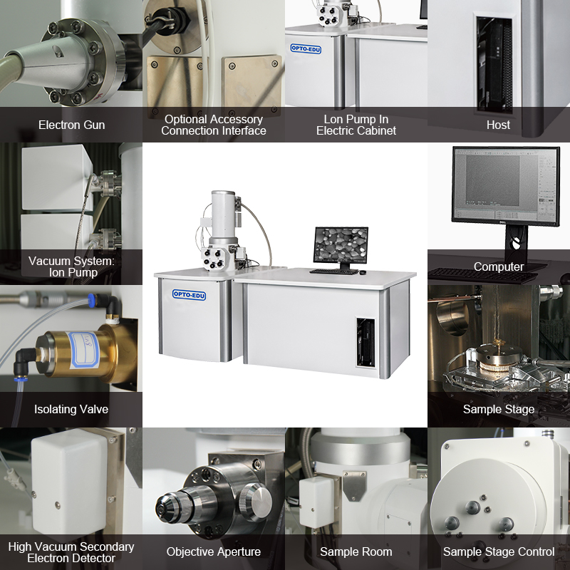
Aperture 3 Molybdenum Objective Apertures, Adjustable Outside Of Vacuum System, No Need Disassemble Objective To Change Aperture 
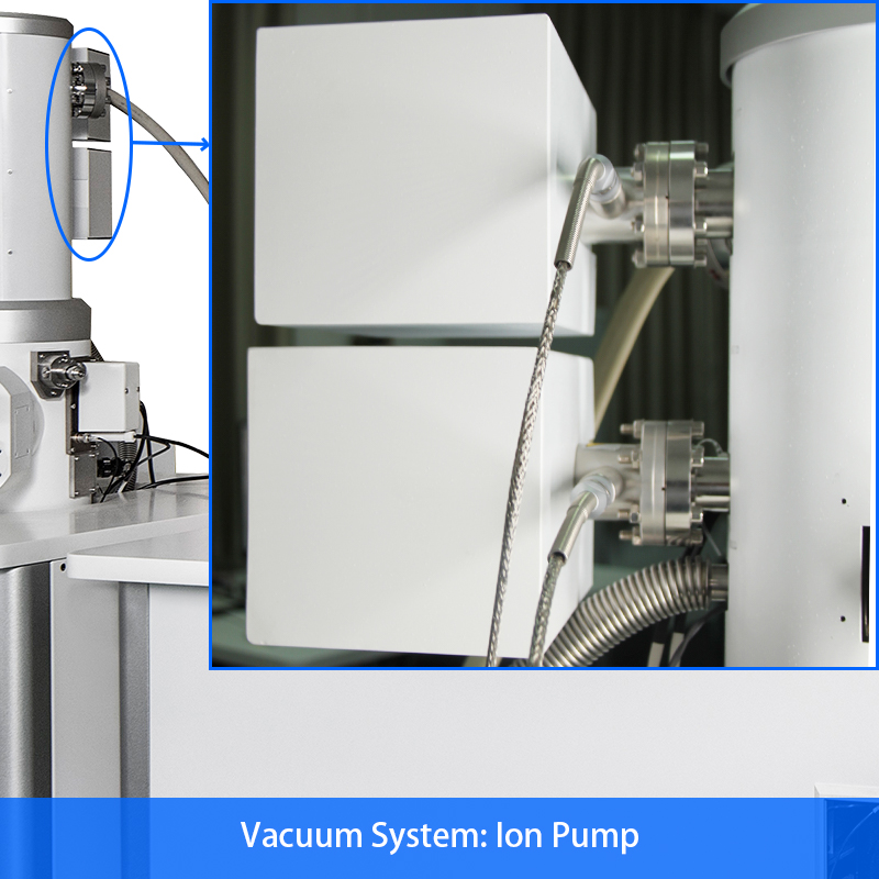
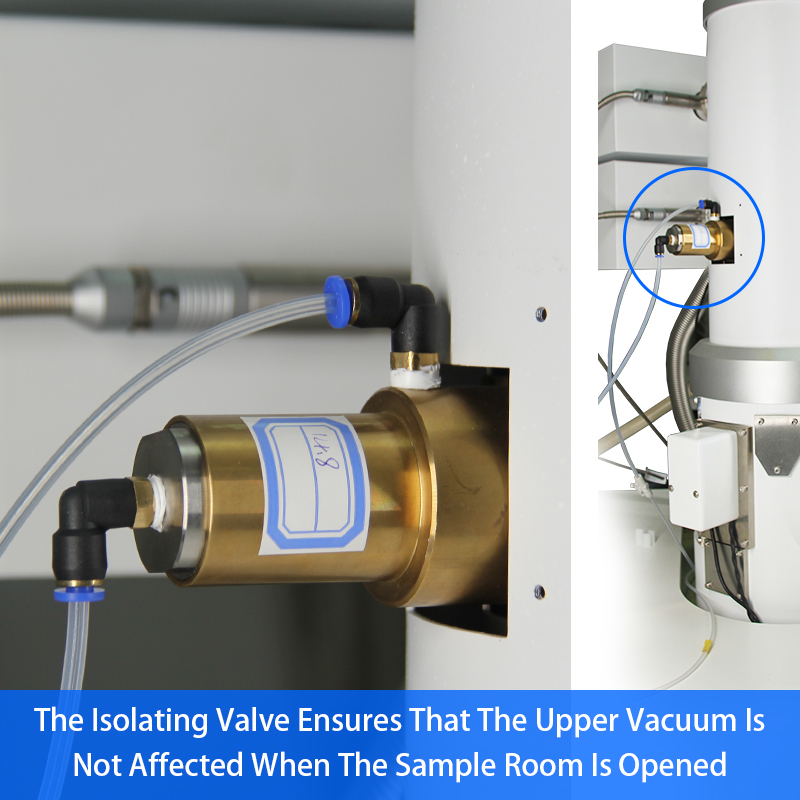
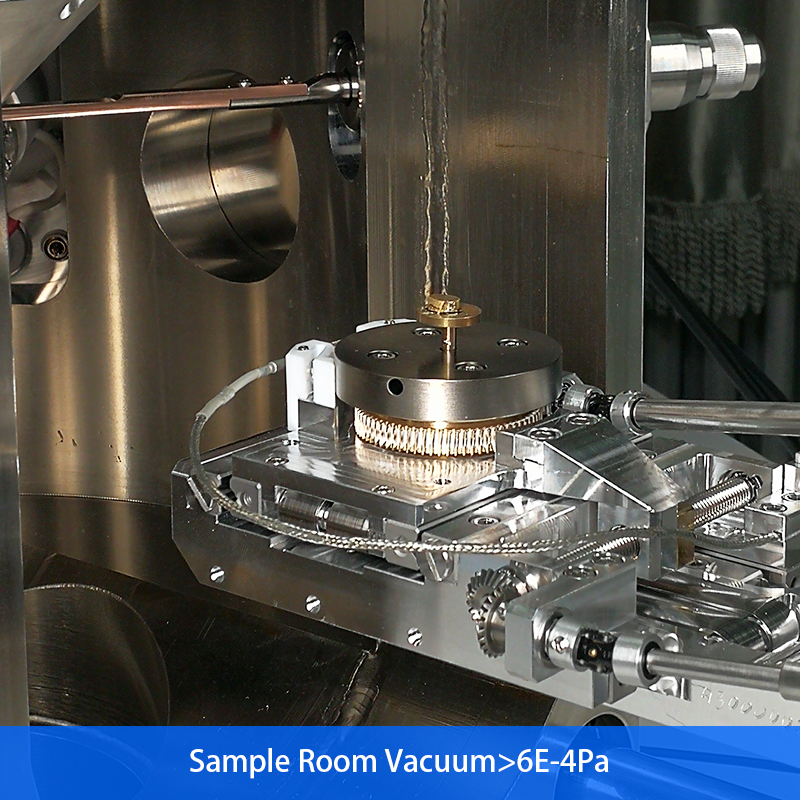
Vacuum System 1 Turbo Molecular Pump1 Mechanical Pump Sample Room Vacuum>2.6E-3Pa Electron Gun Room Vacuum>2.6E-3Pa Fully Auto Vacuum Control Vacuum Interlock Function Optional Model: A63.7069-LV 1 Turbo Molecular Pump 2 Mechanical Pumps Sample Room Vacuum>2.6E-3Pa Electron Gun Room Vacuum>2.6E-3Pa Fully Auto Vacuum Control Vacuum Interlock Function Low Vacuum Range 10~270Pa For Quick Switch in 90 Seconds For BSE(LV)  1 Ion Pump Set1 Turbo Molecular Pump 1 Mechanical Pump Sample Room Vacuum>6E-4Pa Electron Gun Room Vacuum>2E-7 Pa Fully Auto Vacuum Control Vacuum Interlock Function 1 Sputter Ion Pump1 Getter Ion Compound Pump 1 Turbo Molecular Pump 1 Mechanical Pump Sample Room Vacuum>6E-4Pa Electron Gun Room Vacuum>2E-7 Pa Fully Auto Vacuum Control Vacuum Interlock Function
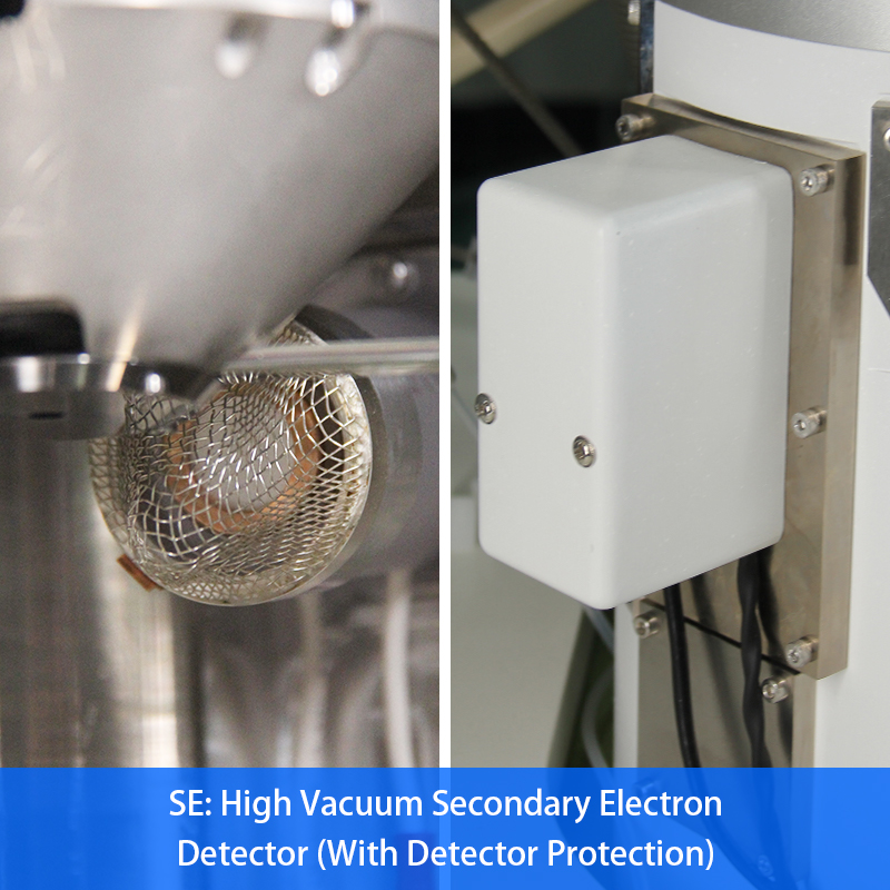
Detector SE: High Vacuum Secondary Electron Detector (With Detector Protection) SE: High Vacuum Secondary Electron Detector (With Detector Protection) SE: High Vacuum Secondary Electron Detector (With Detector Protection)
BSE: Semiconductor 4 SegmentationBack Scattering Detector Optional Model: A63.7069-LV BSE(LV): Semiconductor 4 Segmentation Back Scattering Detector Optional Optional
CCD: Infrared CCD Camera CCD: Infrared CCD Camera CCD: Infrared CCD Camera
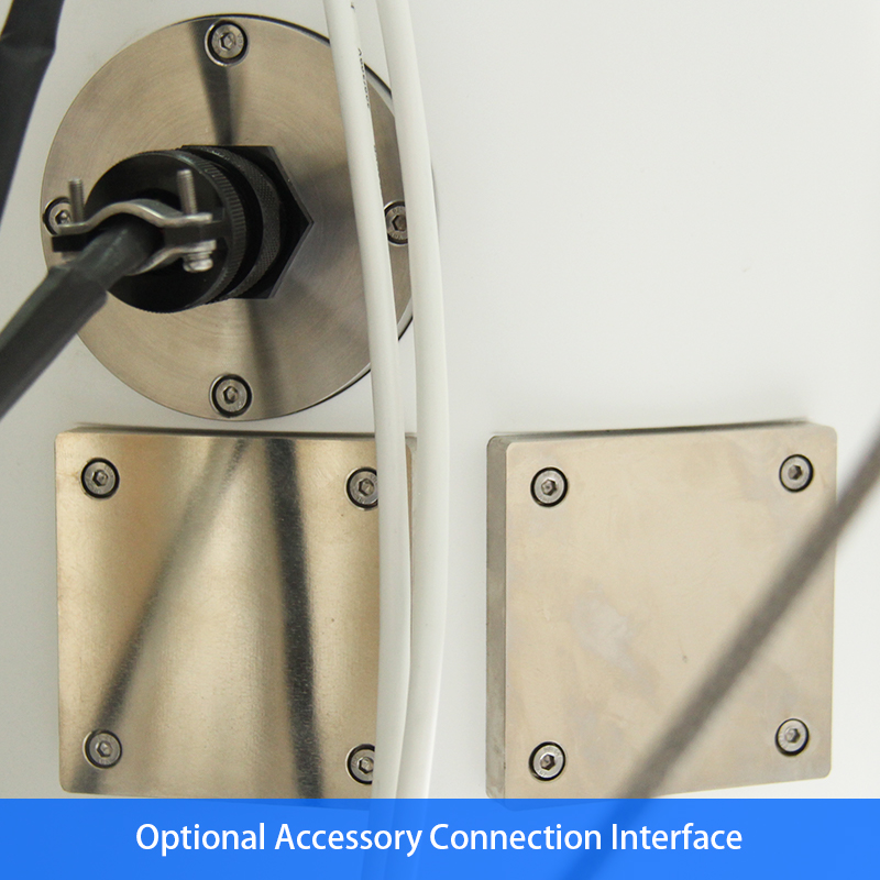
Extend Port 2 Extend Ports On Sample Room ForEDS, BSD, WDS etc. 4 Extend Ports On Sample Room ForBSE, EDS, BSD, WDS etc. 4 Extend Ports On Sample Room ForBSE, EDS, BSD, WDS etc.
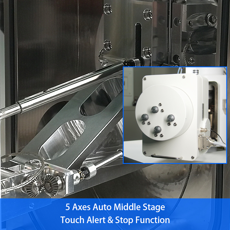
Specimen Stage 5 Axes Stage, 4 Auto +1 Manual ControlTravel Range: X=70mm, Y=50mm, Z=45mm, R=360°, T=-5°~+90°(Manual) Touch Alert & Stop Function 5 Axes Auto Middle StageTravel Range: X=80mm, Y=50mm, Z=30mm, R=360°, T=-5°~+70° Touch Alert & Stop Function Optional Model: A63.7080-M 5 Axes Manual Stage A63.7080-L 5 Axes Auto Large Stage 5 Axes Auto Large StageTravel Range: X=150mm, Y=150mm, Z=60mm, R=360°, T=-5°~+70° Touch Alert & Stop Function
Max Specimen Dia.175mm, Height 35mm Dia.175mm, Height 20mm Dia.340mm, Height 50mm
Image System Real Still Image Max Resolution 4096x4096 Pixels,Image File Format: BMP(Default), GIF, JPG, PNG, TIF Real Still Image Max Resolution 16384x16384 Pixels,Image File Format: TIF(Default), BMP, GIF, JPG, PNG Video: Auto Record Digital .AVI Video Real Still Image Max Resolution 16384x16384 Pixels,Image File Format: TIF(Default), BMP, GIF, JPG, PNG Video: Auto Record Digital .AVI Video
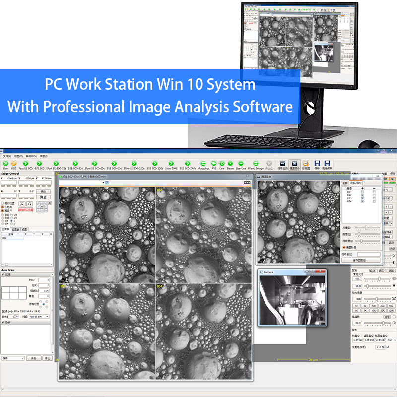
Computer & Software PC Work Station Win 10 System, With Professional Image Analysis Software To Fully Control Whole SEM Microscope Operation, Computer Specification No Less Than Inter I5 3.2GHz, 4G Memory, 24" IPS LCD Monitor, 500G Hard Disk, Mouse, Keyboard
Photo Display The Image Level Is Rich And Meticulous, Showing Real Time Magnification, Ruler, Voltage, Gray Curve
Dimension& Weight Microscope Body 800x800x1850mmWorking Table 1340x850x740mm Total Weight 400Kg Microscope Body 800x800x1480mmWorking Table 1340x850x740mm Total Weight 450Kg Microscope Body 1000x1000x1730mmWorking Table 1330x850x740mm Total Weight 550Kg
Optional Accessories
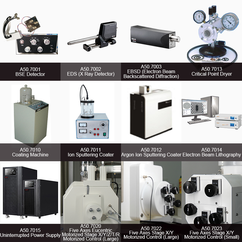
Optional Accessories A50.7002 EDS Energy Dispersive X-Ray SpectrometerA50.7011 Ion Sputtering Coater A50.7001 BSE Back Scattering Electron DetectorA50.7002 EDS Energy Dispersive X-Ray Spectrometer A50.7011 Ion Sputtering Coater A50.7030 Motorize Control Panel A50.7001 BSE Back Scattering Electron DetectorA50.7002 EDS Energy Dispersive X-Ray Spectrometer A50.7011 Ion Sputtering Coater A50.7030 Motorize Control Panel
A50.7001 BSE Detector Semiconductor Four Segment Back Scattering Detector;Available In Ingredients A+B, Morphology Info A-B; Available Sample Observe Without Sputtering Gold; Available In Observe Impurity And Distribution From Grayscale Map Directly.
A50.7002 EDS (X Ray Detector) Silicon Nitride (Si3N4) Window To Optimize Low Energy X-ray Transmission For Light Element Analysis;Excellent Resolution And Their Advanced Low-noise Electronics Provide Outstanding Throughput Performance; The Small Footprint Offers Flexibility To Ensure Ideal Geometry And Aata Collection Conditions; The Detectors Contain A 30mm2 Chip.
A50.7003 EBSD (Electron Beam Backscattered Diffraction) user could analysis crystal orientation, crystal phase and micro texture of materials and related materials performance,etc.automatic optimization of EBSD camera settings during the data collection, do interactive real-time analysis  to obtain maximum information all the data were branded with time tag, which can be viewed at any time high resolution 1392 x 1040 x 12 Scanning and index speed: 198 points / sec, with Ni as the standard, under the condition of 2~5nA, it can ensure the index rate ≥99%; works well under the condition of low beam current and low voltage of 5kV at 100pA orientation measuring accuracy: Better than 0.1 degrees Using triplex index system: no need rely on single band definition , easy indexing of poor pattern quality dedicated database: EBSD special database obtained by electron diffraction: >400 phase structure Index ability: it can automatically index all crystal materials of 7 crystal systems. The advanced options include calculating elastic stiffness (Elastic Stiffness), Taylor (Taylor) factor, Schmidt (Schmid) factor and so on.
A50.7010 Coating Machine Glass Protecting Shell: ∮250mm; 340mm High;Glass Processing Chamber: ∮88mm; 140mm High, ∮88mm; 57mm High; Specimen Stage Size: ∮40mm (max); Vacuum System:molecula Pump And Mechanical Pump; Vacuum Detection: Pirani Gage; Vacuum:better Than 2 X 10⁻³ Pa; Vacuum Protection:20 Pa With Microscale Inflation Valve; Specimen Movement: Plane Rotation,tilt Precession.
A50.7011 Ion Sputtering Coater Glass Processing Chamber: ∮100mm; 130mm High;Specimen Stage Size: ∮40mm( Hold 6 Specimen Cups) ; Golden Target Size: ∮58mm*0.12mm(thickness); Vacuum Detection: Pirani Gage; Vacuum Protection:20 Pa With Microscale Inflation Valve; Medium Gas:argon Or Air With Argon Gas Special Air Inlet And Gas Regulating In Microscale.
A50.7012 Argon Ion Sputtering Coater The Sample Was Plated With Carbon And Gold Under High Vacuum;Rotatable Sample Table, Uniform Coating, Particle Size About 3-5nm; No Selection Of Target Material, No Damage To Samples; The Functions Of Ion Cleaning And Ion Thinning Can Be Realized.
A50.7013 Critical Point Dryer Inner Diameter: 82mm, Inner Length: 82mm;Pressure Range:0-2000psi; Temperature Range:0°-50° C (32°-122° F)
A50.7014 Electron Beam Lithography Based On Scanning Electron Microscope, A Novel Nano-exposure System Was Developed;The Modificaton Has Kept All The Sem Functions For Making Nanoscale Line Width Image; The Modificated Ebl System Widly Applied Into Microelectronic Devices, Optoelectronic Devices, Quantun Devices, Microelectronics System R&d.
A63.7080, A63.7081 Standard Consumables Outfit
1 Field Emission Filament Installed In Microscope 1 Pc
2 Sample Cup Dia.13mm 5 Pcs
3 Sample Cup Dia.32mm 5 Pcs
4 Carbon Double-sided Conductive Tape 6mm 1 Package
5 Vacuum Grease   10 Pcs
6 Hairless Cloth   1 Tube
7 Polishing Paste   1 Pc
8 Sample Box   2 Bags
9 Cotton Swab   1 Pc
10 Oil Mist Filter   1 Pc
A63.7080, A63.7081 Standard Tools & Parts Outfit
1 Inner Hexagon Spanner 1.5mm~10mm 1 Set
2 Tweezers Length 100-120mm 1 Pc
3 Slotted Screwdriver 2*50mm, 2*125mm 2 Pcs
4 Cross Screwdriver 2*125mmm 1 Pc
5 Clean vent pipe Dia.10/6.5mm(Out Diameter/Inner Diameter) 5m
6 Vent pressure reducing valve Output Pressure 0-0.6MPa 1 Pc
7 Internal baking power supply 0-3A DC 2 Pcs
8 UPS power supply 10kVA 2 Pcs
 

Contact us

Please feel free to give your inquiry in the form below We will reply you in 24 hours